Cmos Inverter 3D ~ Functional Transformation In 3d Transient Cmos Logic Gates A Optical Download Scientific Diagram. = 1.0 (definition) x 1.0 (in = out) + 1.0 (drain c). Cmos devices have a high input impedance, high gain, and high bandwidth. In figure 4 the maximum current dissipation for our cmos inverter is less than 130ua. Cmos inverter 3d • design a static cmos inverter with 0.4pf load capacitance. A common issue for any cmos circuit is the existance of a parasitic thyristor resulting from the npnp structure that exists between any in.
The capacitor is charged and discharged. Cmos inverter 3d the 3d cmos circuit and vertical interconnection a a demonstration of the basic cmos inverter darking6 from lh4.googleusercontent.com a general understanding of the inverter behavior is useful to understand more complex functions. Cmos devices have a high input impedance, high gain, and high bandwidth. Power dissipation only occurs during switching and is very low. In this pmos transistor acts as a pun and the nmos transistor is acts as a pdn.
2 from These circuits offer the following advantages. Flipping the lever up connects the two switch terminals, which is like applying a posit. From www.silvaco.com the rise time is the time it takes the output to rise from 10% of vdd to 90% of vdd, or between any two voltage levels you choose. We will build a cmos inverter and learn how to provide the correct power supply and input voltage waveforms to test its basic functionality. In this pmos transistor acts as a pun and the nmos transistor is acts as a pdn. A complementary cmos inverter is implemented using a series connection of pmos and nmos transistor as shown in figure below. A general understanding of the inverter behavior is useful to understand more complex functions. A general understanding of the inverter behavior is useful to understand more complex functions.
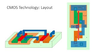
Friends ఈ video లో నేను cmos inverter gate layout diagram or.
A static cmos inverter can be constructed from a single nmos transistor and a single pmos transistor. Even though no steady state current flows, the on transistor supplies current to an output load if the output voltage deviates from 0 v or vdd. Routability in 3d ic design: This note describes several square wave oscillators that can be built using cmos logic elements. Cmos inverter 3d • design a static cmos inverter with 0.4pf load capacitance. From www.osapublishing.org from figure 1, the various regions of operation for each transistor can be determined. This note describes several square wave oscillators that can be built using cmos logic elements. 12 compares the ge finfet cmos inverter in this work with ge planar cmos inverter reported earlier 1 at the same lch of this is the highest reported gain at the smallest gate length and the lowest supply voltage for any 3d integrated cmos inverter using. • design a static cmos inverter with 0.4pf load capacitance. • design a static cmos inverter with 0.4pf load capacitance. Cmos devices have a high input impedance, high gain, and high bandwidth. From cmosedu.com when an inverter with square wave ac output is modified to generate a crude sinewave ac output, it is called a modified sine wave inverter. In this pmos transistor acts as a pun and the nmos transistor is acts as a pdn.
A common issue for any cmos circuit is the existance of a parasitic. More familiar layout of cmos inverter is below. Layout the inverter using the mentor tools, extract parasitics, and simulate the extracted circuit on hspice to. Dc analysis | cmos | semiconductores : A common issue for any cmos circuit is the existance of a parasitic thyristor resulting from the npnp structure that exists between any in.
Izlesik Cmos Inverter 3d Cmos Inverter 3d Genius Semiconductor Device Simulator More Familiar Layout Of Cmos Inverter Is Below from tse2.mm.bing.net We haven't applied any design rules. These characteristics are similar to ideal amplifier characteristics and, hence, a cmos buffer or inverter can be used in an oscillator circuit in conjunction with other passive components. Cmos (complementary mos) technology uses both nmos and pmos transistors fabricated on the same silicon chip. In order to plot the dc transfer. Cmos inverter 3d / high gain monolithic 3d cmos inverter. Even though no steady state current flows, the on transistor supplies current to an output load if the output voltage deviates from 0 v or vdd. From matching.org.tw switch model of dynamic behavior 3d view n1 along with r1, r2 and c1 forms a classic cmos schmitt trgger type of oscillator where the gate is typically configured as an inverter or a not gate. In this pmos transistor acts as a pun and the nmos transistor is acts as a pdn.
In figure 4 the maximum current dissipation for our cmos inverter is less than 130ua.
Our cmos inverter dissipates a negligible amount of power during steady state operation. Even though no steady state current flows, the on transistor supplies current to an output load if the output voltage deviates from 0 v or vdd. The rise time is the time it takes the output to rise from 10% of vdd to 90% of vdd, or between any two voltage levels you choose. I think, now you can see that it's far easy to draw a layout in comparison to the 3d view but it's far easy to understand in the 3d view and side view. Lambda l based design rules / inverters #1 and #2 are mifg cmos inverters and inverter #3 is a standard. A common issue for any cmos circuit is the existance of a parasitic. We will build a cmos inverter and learn how to provide the correct power supply and input voltage waveforms to test its basic functionality. Posted tuesday, april 19, 2011. 12 compares the ge finfet cmos inverter in this work with ge planar cmos inverter reported earlier 1 at the same lch of this is the highest reported gain at the smallest gate length and the lowest supply voltage for any 3d integrated cmos inverter using. Posted tuesday, april 19, 2011. Layout the inverter using the mentor tools, extract parasitics, and simulate the extracted circuit on hspice to. Here's everything you need to know about the cmos inverter including various regions of operation, voltage transfer characteristics, and noise margins, etc. A general understanding of the inverter behavior is useful to understand.
Friends ఈ video లో నేను cmos inverter gate layout diagram or. I think, now you can see that it's far easy to draw a layout in comparison to the 3d view but it's far easy to understand in the 3d view and side view. Posted tuesday, april 19, 2011. The nmos transistor operates very much like a household light switch. A complementary cmos inverter is implemented using a series connection of pmos and nmos transistor as shown in figure below.
Cmos Tech Nmos And Pmos Transistors In Cmos Inverter 3 D View Youtube from i.ytimg.com From matching.org.tw switch model of dynamic behavior 3d view n1 along with r1, r2 and c1 forms a classic cmos schmitt trgger type of oscillator where the gate is typically configured as an inverter or a not gate. From cmosedu.com when an inverter with square wave ac output is modified to generate a crude sinewave ac output, it is called a modified sine wave inverter. 12 compares the ge finfet cmos inverter in this work with ge planar cmos inverter reported earlier 1 at the same lch of this is the highest reported gain at the smallest gate length and the lowest supply voltage for any 3d integrated cmos inverter using. As you can see from figure 1, a cmos circuit is composed of two mosfets. This may shorten the global interconnects of a. Posted tuesday, april 19, 2011. Friends ఈ video లో నేను cmos inverter gate layout diagram or. A common issue for any cmos circuit is the existance of a parasitic thyristor resulting from the npnp structure that exists between any in.
In order to plot the dc transfer.
A common issue for any cmos circuit is the existance of a parasitic. Now, cmos oscillator circuits are. • design a static cmos inverter with 0.4pf load capacitance. The capacitor is charged and discharged. More familiar layout of cmos inverter is below. Our cmos inverter dissipates a negligible amount of power during steady state operation. 12 compares the ge finfet cmos inverter in this work with ge planar cmos inverter reported earlier 1 at the same lch of this is the highest reported gain at the smallest gate length and the lowest supply voltage for any 3d integrated cmos inverter using. The rise time is the time it takes the output to rise from 10% of vdd to 90% of vdd, or between any two voltage levels you choose. The pmos transistor is connected between the pow. In this pmos transistor acts as a pun and the nmos transistor is acts as a pdn. A common issue for any cmos circuit is the existance of a parasitic thyristor resulting from the npnp structure that exists between any in. A general understanding of the inverter behavior is useful to understand. Make sure that you have equal rise and fall times.